


The real bottleneck in GPU manufacturing
H100s make up less than 5% of TSMC's fabrication capacity, so what is it?

What is the bottleneck to producing more GPUs, specifically H100s?
Here are three basic parts of making a GPU1:
Silicon Wafer Production
Producing the silicon wafers on which the chips are made.
Die Fabrication
Includes conducting lithography, deposition, and etching on the silicon wafers. This is to produce dies, which are the most important part of a chip and can be thought of as the brains.
Packaging
Takes dies from a wafer and places them within a package. This then makes a chip. In other words, packaging puts the brain into a skull and gives it a body with a nervous system and muscles to interact with the world.
So where do the bottlenecks lie?
Fabrication and Wafer production
Die fabrication and wafer production are tightly coupled, and we can investigate them together. Some simple math will do here. Each wafer can yield 28 working H100 dies. It is projected 2 million H100s will be produced in 2024, so that turns out to be just above 70,000 wafers.
70,000 is only 5% of TSMC’s 5nm node, which is the process node the H100 is based off of. This means data center GPUs comprise a relatively small amount of TSMC’s capacity.
This number was surprisingly small to me. When all we hear about GPUs, one forgets all the other customers TSMC has, including Apple. Indeed Apple is such a large customer that they absorbed 90% of TSMC’s 3nm capacity last year. That is a lot of iPhones. This is possible because TSMC allocates capacity partly through a bidding system.
If GPU supply is bottlenecked by fabrication, all Nvidia needs to do to expand supply is to place higher bids on TSMC’s capacity — they have the margins to support doing this. They have not, though, and you read the title of this piece, so let’s dig into what is really going on.
Packaging is the bottleneck
How Packaging works
After a die is cut from a wafer, it goes through a variety of steps that “package” it into a chip. This completed form has the die as the central part, and other supporting parts like memory and interconnects surrounding it. Packaging is important because it can allow a chip to receive power and inputs, and transmit outputs. Packaging also takes care of thermal management, heat dissipation, mehcanical protection, chemical contamination, and light exposure.
Packaging can take many different forms depending on the chip. An iPhone chip is packaged differently than a GPU. GPUs need to retrieve inference and training data quickly. Since the models are huge in size, GPUs need a lot of memory and bandwidth. This is why, surrounding the main die of an H100, there are several high bandwidth memory (HBM) components. The HBM and the die are connected together through the package.

HBM allows you to get a lot of bandwidth in a small footprint with great power efficiency, but has some drawbacks. For example, to achieve the fast speeds at the scale that is required, the pads that are used to connect the die to the rest of the circuit need to be very small and connect to short traces (such that the signal does not travel far). The requirements are so steep that only one form of packaging is sufficient: Chip on Wafer on Substrate (CoWoS). It essentially looks like this:
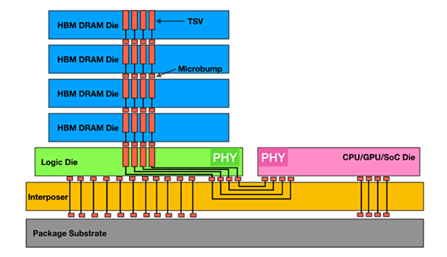
There are a lot of parts to this image, but we can focus on the basic concept: the die is right next to the HBM, and that is placed on a silicon interposer, which is then connected on a packaging substrate (hence the name: chip on wafer on substrate). This then can be placed on a circuit board and connected to other things (power, other chips, etc.).
The problem is twofold: HBM and CoWoS packaging capacities are low. Whenever you hear demand outstrips supply, these are the culprits.
Unlike traditional packaging, which happens at separate facilities from fabrication, only TSMC does CoWoS packaging in-house. It is a complicated process that involves a huge amount of vendors, specialized facilities, and special training for personnel. While TSMC has been increasing their capacity, they have not developed large enough capacity for the high demand as of the time of writing. My guess is that they did not anticipate this sort of demand, and even if they did, it is difficult to meet it at the speed in which it came.
I think one part that helps ground this for me is that a recently announced packaging facility is 12 hectares in size, requires 3,000 skilled workers to function, and is expected to be completed by the end of 2026. We are dealing with numbers and facilities so large it is difficult to comprehend, and I think saying “there is not enough capacity to meet demand” does not get across the sheer amount of work needed to reach the required capacity. This, in many ways, is a megaproject necessitating engineering marvels to pull of. Nevertheless, TSMC is aggressively expanding their capacity and building many more facilities in Taiwan (though some reports can be exaggerated to prop up land value). TSMC’s CoWoS packaging is expected to process around 33,000-35,000 wafers per month by the end of 2024, equivalent to just above 900,000 H100 chips. Even if this estimate is off, as TSMC will probably be packaging Nvidia’s next generation chip by the end of 2024, TSMC is on track to increase packaging capacity by 60% annually through to 2026. By then, projected yeilds are around 60,000 - 70,000 wafers per month. It is perhaps worth mentioning that this next generation chip allows for packaging two dies on the same chip, so that might change estimates.
HBM production shortage
Much like everything else in this industry, there is one main supplier and several others trailing behind — SK Hynix has somewhere between 50-70% market share of HBM and is Nvidia’s main supplier for H100’s HBM. SK Hynix is also the primary supplier for Meta, AMD, Google, and Intel.
The South Korean company is sold out on HBM till 2026. It is not clear to me why they are so constrained on capacity. My guess is that the reason is not complicated: no one anticipated there being this much demand for HBM this fast. The facilities needed to produce HBM are also difficult to make and require lots of resources, time to build, and training for personnel.
Why not use something other than HBM? My understanding is that HBM is the only form of memory that can give a reasonable power profile in addition to the required bandwidth. It is also cheaper compared to other forms of memory like SRAM. I imagine there are other more tacit reasons for picking HBM, but they are probably detailed in some internal Nvidia documentation.
As for the future, both Micron and SK Hynix are aggressively expanding production capacity. The goal is to be able to produce as many HBMs as possible. Analysts estimate 45% annual growth between now and 2030. More recent news came out that SK Hynix was awarded CHIPS Act grant money, and with the recent success in Arizona, I would not be surprised if HBM supply grew faster than 45% annually.
Expansion and future outlook
GPU production is bottlenecked by HBM and CoWoS packaging capacity. Increasing this capacity is the hardest part of ramping up production, and as soon as that is done, I predict that die fabrication for GPUs will become an increasing part of TSMC’s fab capacity at the 3nm node. Recently announced expansions include contracting out CoWoS packaging to American companies like Amok, which is a unique and noteworthy development. Amok is also a CHIPS Act recipient.
Given these expansions, we could see GPU production be enough to sustain training runs with at least tens of millions of H100 equivalent GPUs by 2030, going up to 400 million H100 equivalents.
Thanks to Emily Nobes for helpful feedback.
Standard caveats apply: this is highly simplified for the purposes of this article, reality is way more complicated, etc.