
How do Google's AI chips stack up against Nvidia's?
Nvidia's market share is safe, but it is closer than you think!

In an era of Nvidia hegemony, Google has been a holdout for over a decade. The chips on which they train and do inference, called Tensor Processing Units (TPUs), are designed in-house. Their determination for chip self-reliance is only growing — they recently released their newest chip: TPUv6, or Trillium.
I wanted to dive into how these things work, what makes them different, and if they provide Google an advantage compared to other hyperscalers like Microsoft and Amazon. Importantly, I also want to see if they stand up against NVIDIA’s chips (spoiler, they do) and why people are not flocking to Google given the incredible demand for chips.
Microarchitecture
The TPU is an Application Specific Integrated Chip (ASIC). The application in mind is running transformer models as fast and efficiently as possible through having a specialized architecture. The main parts are:
Large, optimized Matrix Multiply Units (MXUs) for the core tensor operations. This is the main part of the TPU; it does most of the important math. The MXU is set up as a Systolic Array, which helps in efficiency and reduces memory bandwidth requirements.
MXUs are supported by Vector Processing Units and Scalar Computation Units, which handle operations not suitable for the MXU
On-chip memory (including high-bandwidth memory)
A custom Inter-Chip Interconnect (ICI) for scalable multi-chip operations.
This enables low-latency, high-bandwidth communication between TPUs, allowing for easy scaling to thousands of chips, crucial for LLM training.
TPUv6 supports both bf16 and bf8. For more on the architecture, you can read here. In contrast, a single Nvidia H100 uses more power and has an architecture that can accommodate a wider range of workloads, beyond running transformer models. While an H100 has more memory bandwidth, TPUs often have more sophisticated on-chip memory hierarchies optimized specifically for AI workloads. Finally, an H100 uses Nvidia’s interconnect system, which includes NVLink, NVSwitch, and Infiniband to enable high-speed communication between GPUs. While it boasts impressive speeds, Google’s custom ICI system is specifically designed for AI workloads and so is better suited for large data center operations (e.g., it requires fewer switches as chips scale than Nvidia and is cheaper).
In terms of pure computational power, TPUs have held up against GPUs on a per-chip basis.
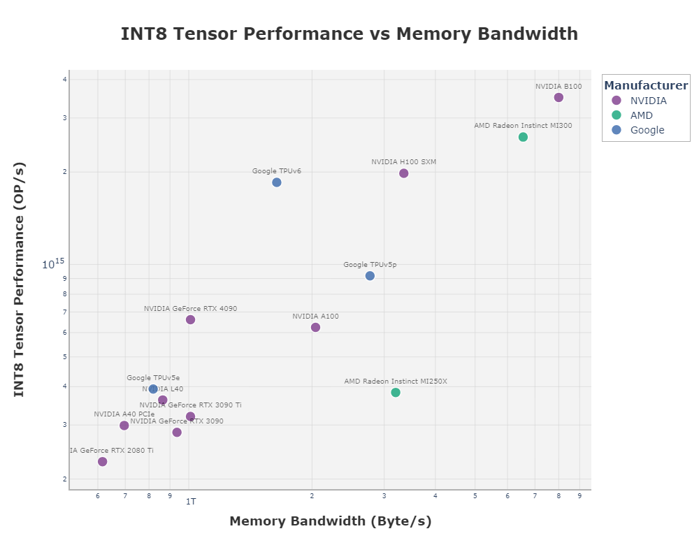
Note that the TPU v5e was an inference-based chip, while the TPU v5p is training-focused. The tricky part about these comparisons are not exactly apples to apples. Nvidia’s GPUs use more power per chip so it makes sense they are more powerful.
It is interesting to note that although Trillium was released in May of 2024, it has probably been in use for over a year internally, as is indicated by a court case over alleged espionage. This means the gap between Nvidia and Google’s designs is closer than what would initially seem (my guess is around just under one year).
In any case, a lot of these microarchitecture changes make a big difference when it comes to scaling these chips out to the tens or hundreds of thousands, and that will be examined in the next section. But first, a brief look from the world of software.
The software ecosystem that these chips exist in is very important. AMD’s chips have very solid specs, but due to the incredibly difficult-to-operate software ecosystem, barely anyone uses them. Google similarly has a lacking external software ecosystem (posts like this are not uncommon), but it is better than AMD’s. NVIDIA’s CUDA ecosystem, on the other hand, is perhaps more defensible than its hardware. It is the industry standard and what many people already know how to use and build on. Nvidia made an early bet on CUDA and grew the ecosystem to have many convenient functions and tools, which are generally well-documented. The software ecosystem is not a large focus of this piece, but may contribute to why you have not heard people talk about Google’s TPUs as much!
Counting up the chips
The most recent TPU (Trillium) can scale to 256 chips per “pod”. Within the pod, they are connected via ICI and then the pods can be scaled way up into the hundreds. To connect all the pods, Google developed its own custom optical switches, which reduced cost by 30%, used 40% less power, and provided 50x less downtime. This can quickly end up connecting tens of thousands of chips, or even hundreds of thousands. Combined with Google using a special network topology to reduce latency, TPUs are easier to scale than Nvidia’s H100 chips.
At large scales of use and energy, small gains in efficiency make a huge difference (recall: xAI’s data center uses as much energy as ~100k homes) and Google is really good at building efficient data centers. Their data centers are 30% more efficient than Microsoft’s, and have industry-leading numbers in terms of overall efficiency. Combined with TPU’s higher efficiency as a chip, Google has a huge lead in infrastructure as it relates to data center build-out and utilization. Given that energy is expected to be a bottleneck, this may give Google a slight edge. However, competitors like Microsoft are reviving nuclear power plants, so the race continues to be close.
Google has been building data centers for a long time, and that knowledge has become useful. Google has developed custom silicon to manage and maintain its giant pods (security, load management), which were originally designed for its cloud CPU offerings. This know-how is, I suspect, why they have been the only hyperscaler (as of the time of writing) to pull off a training run across different data centers.
Scaling also faces emergent challenges. Take fault tolerance: if one GPU or one GPU/TPU experiences an error then the entire cluster must restart from a checkpoint, leading to a large amount of idle time on expensive machines. Fault tolerance allows you to deal with this such that only neighbouring GPUs are temporarily affected. NVIDIA’s protocols seemingly fail to solve this problem sufficiently at a massive scale, so many labs have had to develop their own methods.
Google, however, has developed a large amount of fault tolerance methods, and indeed, employs the top experts on the topic. I expect this to be a significant advantage for Google.
Because Google is integrating vertically — designing chips, writing software to manage those chips, building data centers, and then training the models—they can solve systemic problems quickly (bureaucracy permitting) and cheaply. NVIDIA has eye-watering margins (75%) on their data center business, which all hyperscalers have to pay, except Google1. Indeed, it seems NVIDIA is in such high demand that they could get away with a higher margin, but this way, Sundar is not chasing after Jensen.
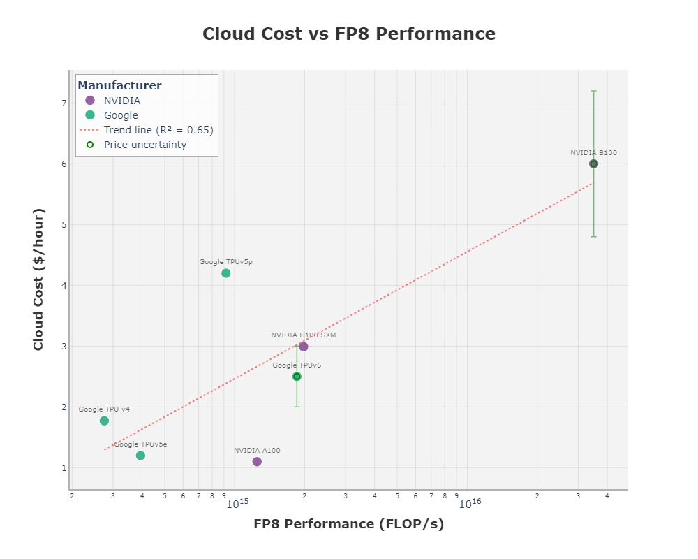
Some have speculated that Google’s TPUs are more expensive per FLOP/s than NVIDIA’s GPUs for the non-Googler consumer. If you are renting them using Google Cloud, this may be true (depending on the version). However, I would guess this has saved Google a ton of money: keep in mind that these TPUs are also used for other purposes, not just foundation models (e.g. real-time voice search). Overall, I think TPUv6 does well in cost per FLOP/s, depending on how the cloud pricing shakes out. Below is some data I collected on the prices as they compare to FP8 performance2. While FP8 may not be what is used on the B100, the comparison is still worth it.
If these chips are as good as they seem, why is no one running to Google to get their hands on them?
Where are all of the TPU customers?
There are existing customers, kind of. Anthropic and Apple both use TPUs for inference and training. Google invested $2B in Anthropic, so it is not exactly a normal customer. As for Apple, there are several reasons why they would go with Google: they have a good relationship (most of iCloud runs on Google Cloud, and Google is the default search engine on Apple), Google has higher availability than NVIDIA, and Apple possibly holds a grudge against NVIDIA.
Google also allows you to use TPUs through their cloud platform, but I suspect it only comprises a small amount of revenue for them.
So, why doesn’t Google have more TPU customers? It doesn’t want the business. It does not make sense for them to commercialize their chips to the extent that NVIDIA does. Unlike NVIDIA, which solely sells hardware, Google also builds foundation models. This means selling TPUs could cannibalize its own supply and give competitors access to an edge they’ve developed.
Plus, commercializing chips requires an entirely different skillset, one that Google has to develop over time. Teams of solution architects must be ready to help customers set up and use these chips, but also technicians and engineers to assist in setting up the data centers. This support infrastructure is crucial for enterprise adoption and is an area where NVIDIA excels due to its long history in the market.
Commercializing also comes with a fundamental trade-off: if they sell their chips, they lose the ability to fully customize their chips to their needs. It would need to cater to different customer configurations, diluting its competitive edge. They would also have to start selling and offering many of their data center innovations, which help the TPU be as good as it is.
With TPUs kept in-house, Google can boast the strong positives of vertically integrating, controlling access to the technology, have tight feedback loops for iterating quickly, while avoiding paying Nvidia margins.
Thanks to Wim Howson-Creutzberg for useful feedback, comments, and conversations.
This is a reason why Microsoft and Amazon are both developing in-house chips for training and inference. Meta has already developed inference chips.
Note the high uncertainty on the B100, as no cloud provider is currently listing their prices for it yet. This is not meant as an authoritative price estimate, just my best guess.